
- All
- Product Management
- News
- Introduction
- Enterprise outlets
- FAQ
- Enterprise Video
- Enterprise Atlas

Xi'an Jiaotong University Successfully Achieve Mass Production of 2-inch Heteroepitaxial Single Crystal Diamond Substrate
Release time:
2024-09-27 15:51
Recently, the entrepreneurial team led by Professor Wang Hongxing of Xi 'an Jiaotong UniversityDiamondSignificant progress and breakthroughs have been made in the industrialization of substrate technology. The team used a microwave-based plasma chemical vapor deposition (MPCVD) technique to achieve a 2-inchHeteroepitaxial Single Crystal Diamond SubstrateThe mass production, this innovative achievement marks our country insuperhard materialThe research in this field has reached the international leading level and will provide strong technical support for the development of related industries.
In the principle of semiconductor preparation, the substrate is a wafer made of semiconductor single crystal material, and different substrate materials can produce semiconductor chips including single crystal diamond. Single crystal diamond is known as the "ultimate semiconductor", and silicon is the same as the elemental semiconductor, performance completely beyond the existing semiconductor, can overcome the "breakdown field strength" and "self-heating effect" bottleneck. In the ultra-high voltage, ultra-large current, ultra-high power, high efficiency, radiation resistance and ultra-high frequency work without cooling of electronic devices, single crystal diamond has unique advantages.
As an expert who has been engaged in the research of single crystal diamond wide band gap semiconductor materials and devices for a long time in China, Wang Hongxing led the team to successfully realize the batch of 2-inch heteroepitaxial single crystal diamond self-supporting substrate after long-term scientific research (as shown in Figure 1). Through the effective control of film uniformity, temperature field and flow field, the yield of heteroepitaxial single crystal diamond is improved. The substrate surface has a step-flow growth mode (as shown in Figure 2), which can reduce the defect density of the substrate and improve the crystal quality. The half-peak widths of the XRD(004) and (311) rocking curves were less than 91 arcsec and 111 arcsec, respectively (as shown in Figure 3).

Figure I. Photo of 2-inch heteroepitaxial single crystal diamond self-supporting substrate
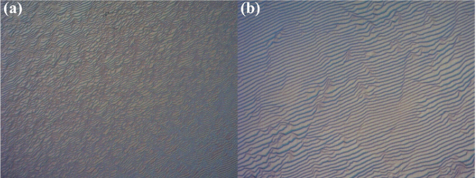
Figure II. Heteroepitaxial diamond optical microscope photo (a) 100 times magnification (B) 500 times magnification

Figure 3. XRD test results (a)(004) face rocking curve; (B)(311) face rocking curve;(c)(311) face four-fold symmetry;(d) pole figure
The method uses microwave plasma to excite the reaction gas to achieve the growth of heteroepitaxial single crystal diamond at lower temperature and pressure. Compared with the traditional preparation method, the method has a higher growth rate and lower cost, and can realize large-scale production. And then effectively ensure the domestic power electronic devices, heat conduction, radar detection and other fields for high-quality, large-size electronic grade single crystal diamond demand, while meeting the needs of scientific research institutions for high-quality seeds.
In addition to scientific applications, this breakthrough also has great potential in the commercial and industrial fields. For example, it may also be applied to the following applications:
Advanced cutting tools: The high hardness and wear resistance of diamond make it an ideal material for manufacturing high-end cutting tools. By using a heteroepitaxial single crystal diamond substrate, a more durable and accurate cutting tool can be manufactured, thereby improving cutting efficiency and reducing production costs.
2. Electronic and semiconductor devices: Diamond's thermal conductivity and electrical insulation make it an ideal material for electronic and semiconductor devices. By using heteroepitaxial single crystal diamond substrates, more efficient and reliable electronic and semiconductor devices can be fabricated.
Optical instruments and lasers: Diamond's high optical transparency and stability make it an ideal material for manufacturing optical instruments and lasers. By using heteroepitaxial single crystal diamond substrates, more accurate and stable optical instruments and lasers can be fabricated.
4. Sensors and detectors: The high sensitivity and stability of diamond make it an ideal material for manufacturing sensors and detectors. By using heteroepitaxial single crystal diamond substrates, more accurate and reliable sensors and detectors can be fabricated.
It is worth mentioning that the industrialization of the research results has broken the foreign technology monopoly, reduced the production cost of domestic related industries, and the application prospect is very broad. With the rapid development of emerging technologies such as 5G and the Internet of Things, the application demand of diamond in the fields of electronics, photons, and quantum is increasing. The mass production of heteroepitaxial single crystal diamond substrate will provide more stable and reliable raw material support for the development of related industries. At the same time, the popularization and application of this achievement will also drive the development of related industrial chains and promote the transformation and upgrading of my country's economy. We look forward to more applications and breakthroughs of this technology in the future.

Concerned about the public.
Copyright©Superhard Materials Branch of China Machine Tool Industry Association